- 您现在的位置:买卖IC网 > Sheet目录472 > MAX2062ETM+ (Maxim Integrated)IC VGA ANALOG/DIGITAL 48TQFN-EP
�� �
�
�Dual� 50MHz� to� 1000MHz� High-Linearity,�
�Serial/Parallel-Controlled� Analog/Digital� VGA�
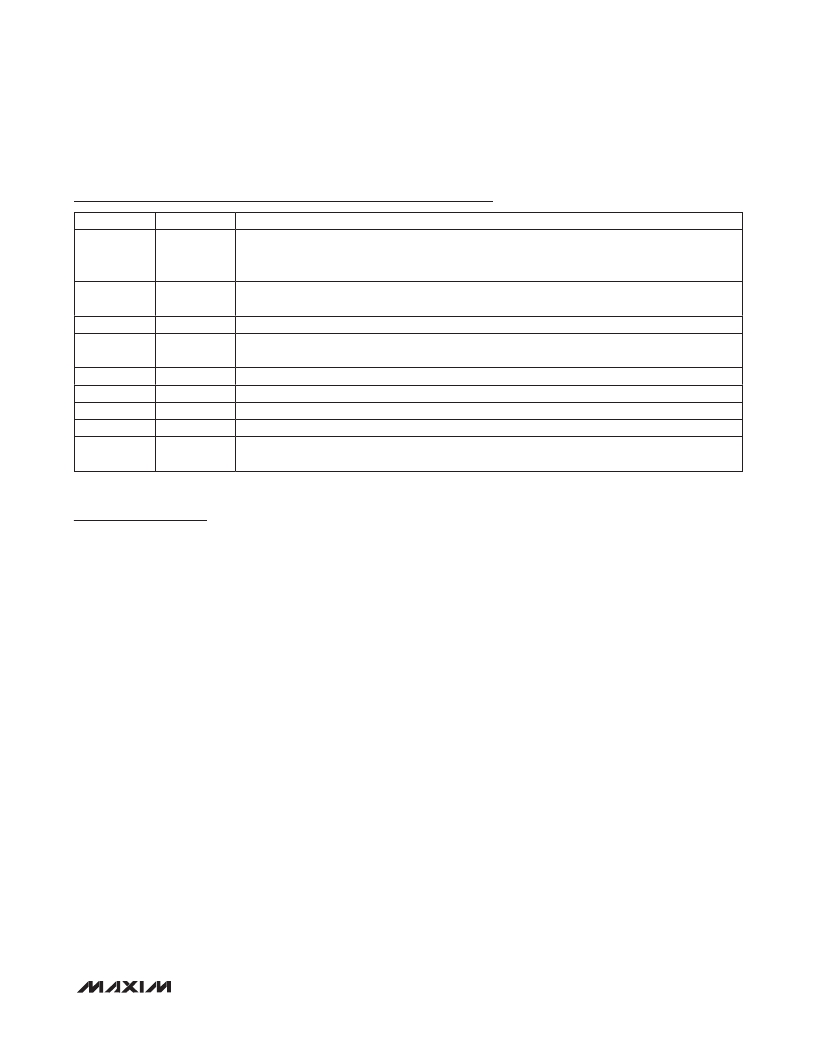
�Pin� Description� (continued)�
�PIN�
�40�
�41�
�42�
�43�
�44�
�45�
�46�
�47�
�—�
�NAME�
�AA_SP�
�A_ATT_IN_1�
�D4_1�
�D_ATT_OUT_1�
�D3_1�
�D2_1�
�D1_1�
�D0_1�
�EP�
�FUNCTION�
�DAC� Enable/Disable� Logic� Input� for� Analog� Attenuators.� Set� AA_SP� to� logic� 1� to� enable� on-chip�
�DAC� circuit� and� digital� SPI� control.� Set� AA_SP� to� logic� 0� to� disable� DAC� circuit� and� digital� SPI�
�control.� When� AA_SP� =� 0,� use� analog� control� lines� (A_VCTL_1� and� A_VCTL_2).�
�Analog� Attenuator� Input� (50� I� ),� Path� 1.� Requires� a� DC-blocking� capacitor.� Connect� to�
�D_ATT_OUT_1� through� a� 1000pF� capacitor.�
�16dB� Attenuator� Logic� Input,� Path� 1.� Logic� 0� =� disable,� logic� 1� =� enable.�
�5-Bit� Digital� Attenuator� Output� (50� I� ),� Path� 1.� Requires� a� DC-blocking� capacitor.� Connect� to�
�A_ATT_IN_1� through� a� 1000pF� capacitor.�
�8dB� Attenuator� Logic� Input,� Path� 1.� Logic� 0� =� disable,� logic� 1� =� enable.�
�4dB� Attenuator� Logic� Input,� Path� 1.� Logic� 0� =� disable,� logic� 1� =� enable.�
�2dB� Attenuator� Logic� Input,� Path� 1.� Logic� 0� =� disable,� logic� 1� =� enable.�
�1dB� Attenuator� Logic� Input,� Path� 1.� Logic� 0� =� disable,� logic� 1� =� enable.�
�Exposed� Pad.� Internally� connected� to� GND.� Connect� to� GND� for� proper� RF� performance� and�
�enhanced� thermal� dissipation.�
�Detailed� Description�
�The� MAX2062� high-linearity� analog/digital� VGA� is� a�
�general-purpose,� high-performance� amplifier� designed�
�to� interface� with� 50� I� systems� operating� in� the� 50MHz� to�
�1000MHz� frequency� range.�
�Each� channel� of� the� device� integrates� one� digital� attenua-�
�tor� and� one� analog� attenuator� to� provide� 64dB� of� total� gain�
�control,� as� well� as� a� driver� amplifier� optimized� to� provide�
�high� gain,� high� IP3,� low� NF,� and� low� power� consumption.�
�Each� digital� attenuator� is� controlled� as� a� slave� periph-�
�eral� using� either� the� SPI-compatible� interface,� or� a� 5-bit�
�parallel� bus� with� 31dB� total� adjustment� range� in� 1dB�
�steps.� An� added� feature� allows� rapid-fire� gain� selection�
�among� each� of� the� four� steps,� preprogrammed� by� the�
�user� through� the� SPI-compatible� interface.� A� separate�
�2-pin� control� lets� the� user� quickly� access� any� one� of� four�
�customized� attenuation� states� without� reprogramming�
�the� SPI� bus.� Each� analog� attenuator� is� controlled� using�
�an� external� voltage� or� through� the� SPI-compatible� inter-�
�face� using� an� on-chip� 8-bit� DAC.� See� the� Applications�
�Information� section� for� attenuator� programming� details.�
�Because� each� of� the� three� stages� in� the� separate� signal�
�paths� has� its� own� RF� input� and� RF� output,� this� compo-�
�nent� can� be� configured� to� either� optimize� NF� (amplifier�
�configured� first),� OIP3� (amplifier� last),� or� a� compromise�
�of� NF� and� OIP3.� The� device’s� performance� features�
�include� 24dB� amplifier� gain� (amplifier� only),� 7.3dB� NF�
�at� maximum� gain� (includes� attenuator� insertion� losses),�
�and� a� high� OIP3� level� of� +41dBm.� Each� of� these� features�
�makes� the� device� an� ideal� VGA� for� multipath� receiver�
�and� transmitter� applications.�
�In� addition,� the� device� operates� from� a� single� +5V�
�supply� with� full� performance,� or� a� +3.3V� supply� for� an�
�enhanced� power-savings� mode� with� lower� performance.�
�The� device� is� available� in� a� compact� 48-pin� TQFN� pack-�
�age� (7mm� x� 7mm)� with� an� exposed� pad.� Electrical� per-�
�formance� is� guaranteed� over� the� extended� temperature�
�range� (T� C� =� -40� N� C� to� +85� N� C).�
�Analog� and� 5-Bit� Digital� Attenuator� Control�
�The� device� integrates� two� analog� attenuators� and� two�
�5-bit� digital� attenuators� to� achieve� a� high� level� of� dynam-�
�ic� range.� Each� analog� attenuator� has� a� 33dB� range�
�and� is� controlled� using� an� external� voltage� or� through�
�the� 3-wire� SPI� interface� using� an� on-chip� 8-bit� DAC.�
�Each� digital� attenuator� has� a� 31dB� control� range,� a� 1dB�
�step� size,� and� is� programmed� either� through� the� 3-wire�
�SPI� or� through� a� separate� 5-bit� parallel� bus.� See� the�
�Applications� Information� section� and� Table� 1� for� attenu-�
�ator� programming� details.� The� attenuators� can� be� used�
�for� both� static� and� dynamic� power� control.�
�Note� that� when� the� analog� attenuators� are� controlled�
�by� the� DACs� through� the� SPI� bus,� the� DAC� output�
�voltage� shows� on� pins� A_VCTL_1� and� A_VCTL_2� (pins�
�39� and� 22,� respectively).� Therefore,� in� SPI� mode,� the�
�A_VCTL_1� and� A_VCTL_2� pins� must� only� connect� to� the�
�resistor� and� capacitor� to� ground,� as� shown� in� the� Typical�
�Application� Circuit� .�
�______________________________________________________________________________________�
�17�
�发布紧急采购,3分钟左右您将得到回复。
相关PDF资料
MAX2063ETM+
IC VGA PROG DIGITAL 48TQFN-EP
MAX2064ETM+
IC VGA PROG ANALOG 48TQFN-EP
MAX2065EVKIT
KIT EVALUATION FOR MAX2065
MAX2066EVKIT
KIT EVALUATION FOR MAX2066
MAX2067EVKIT
KIT EVALUATION FOR MAX2067
MAX2091ETP+T
IC UPCONVERTING MIXER 20TQFN
MAX2092ETP+T
IC UPCONVERTING MIXER 20TQFN
MAX2112EVKIT+
KIT EVAL FOR MAX2112
相关代理商/技术参数
MAX2062ETM+T
功能描述:射频放大器 MAX2062 Eval Kit
RoHS:否 制造商:Skyworks Solutions, Inc. 类型:Low Noise Amplifier 工作频率:2.3 GHz to 2.8 GHz P1dB:18.5 dBm 输出截获点:37.5 dBm 功率增益类型:32 dB 噪声系数:0.85 dB 工作电源电压:5 V 电源电流:125 mA 测试频率:2.6 GHz 最大工作温度:+ 85 C 安装风格:SMD/SMT 封装 / 箱体:QFN-16 封装:Reel
MAX2062EVKIT#
功能描述:放大器 IC 开发工具 MAX2062 Eval Kit
RoHS:否 制造商:International Rectifier 产品:Demonstration Boards 类型:Power Amplifiers 工具用于评估:IR4302 工作电源电压:13 V to 23 V
MAX2063
制造商:MAXIM 制造商全称:Maxim Integrated Products 功能描述:Dual 50MHz to 1000MHz High-Linearity, Serial/Parallel-Controlled Digital VGA
MAX2063ETM+
功能描述:射频放大器 Dl 50-1000MHz Hi-Lin Analog/Digital VGA RoHS:否 制造商:Skyworks Solutions, Inc. 类型:Low Noise Amplifier 工作频率:2.3 GHz to 2.8 GHz P1dB:18.5 dBm 输出截获点:37.5 dBm 功率增益类型:32 dB 噪声系数:0.85 dB 工作电源电压:5 V 电源电流:125 mA 测试频率:2.6 GHz 最大工作温度:+ 85 C 安装风格:SMD/SMT 封装 / 箱体:QFN-16 封装:Reel
MAX2063ETM+T
功能描述:射频放大器 Dl 50-1000MHz Hi-Lin Analog/Digital VGA RoHS:否 制造商:Skyworks Solutions, Inc. 类型:Low Noise Amplifier 工作频率:2.3 GHz to 2.8 GHz P1dB:18.5 dBm 输出截获点:37.5 dBm 功率增益类型:32 dB 噪声系数:0.85 dB 工作电源电压:5 V 电源电流:125 mA 测试频率:2.6 GHz 最大工作温度:+ 85 C 安装风格:SMD/SMT 封装 / 箱体:QFN-16 封装:Reel
MAX2063EVKIT#
功能描述:放大器 IC 开发工具 MAX2063 Eval Kit RoHS:否 制造商:International Rectifier 产品:Demonstration Boards 类型:Power Amplifiers 工具用于评估:IR4302 工作电源电压:13 V to 23 V
MAX2063双通道数字放大器
制造商:未知厂家 制造商全称:未知厂家 功能描述:
MAX2064
制造商:MAXIM 制造商全称:Maxim Integrated Products 功能描述:Dual 50MHz to 1000MHz High-Linearity, Serial/Analog-Controlled VGA